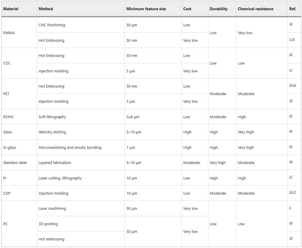
Microfluidic technology has advanced significantly over the past few decades, becoming an irreplaceable part of complex tools in healthcare, environmental monitoring, and chemical engineering. Microfluidic chips, at the heart of this transformative technology, are tiny systems capable of precisely processing small volumes of fluids. The manufacturing technology of these chips greatly impacts their design and performance, with each technology offering unique advantages and limitations. In addition to common manufacturing technologies, the industry has explored several alternative methods, such as thermal embossing, 3D printing, laser ablation, and paper-based microfluidics. For example, heat embossing is suitable for thermoplastic materials, offering high throughput but requiring the initialfabrication of molds. 3D printing, a rapid prototyping technology with high design flexibility, but is often limited by resolution and can be time-consuming. Laser ablation can produce high-precision microchannels, but it is also time-intensive and may induce undesirable thermal effects that change material properties.
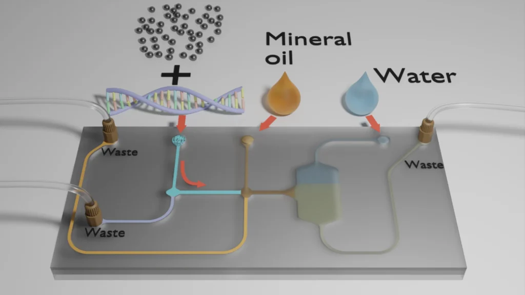 Schematic diagram of a microfluidic chip design
Nevertheless, laser ablation has been widely used in large-scale mass-production of microfluidic chips for applications such as electrochemical glucose monitoring and biomarker detection. Paper-based microfluidics are extremely cost-effective and portable but are generally limited to simpler detection and fluid manipulation. As the application of microfluidic devices expands, there is a growing need to understand the advantages and disadvantages of different manufacturing technologies.
Layered stainless steel manufacturing involves stacking and connecting metal layers to build complex microchannel networks. This technology benefits from the material’s durability and resistance to harsh conditions, making it suitable for high-pressure or high-temperature applications. It can also achieve micron-level precision. However, the process is costly due to the metal processing and bonding technologies involved.
Polyimide is a high-performance polymer with excellent chemical resistance and thermal stability, and is commonly used as a substrate in microfluidic applications. Polyimide is usually molded into the required microfluidic structure using techniques such as laser cutting and photolithography. These methods can produce flexible and heat-resistant microfluidic chips, but the manufacturing process is quite complicated. Compared to MEMS micromachining-based methods, polyimide’s microchannel surface roughness is high, and the size of the microchannels cannot be precisely controlled.
Silicon-glass devices are usually anodically bonded, which provides excellent chemical resistance and optical transparency. These devices are ideal for applications that require high temperatures or exposure to corrosive chemicals. However, their high production costs and long manufacturing cycles limit their applicability in rapid prototyping or low-cost applications.
Soft lithography, especially for polydimethylsiloxane (PDMS) devices, is a pioneering technology that perfectly combines flexibility, biocompatibility, and rapid prototyping capabilities. PDMS devices are widely used in biological fields due to their inertness and low absorption rate for small molecules. Although they are a popular choice in microfluidic chip manufacturing, PDMS materials have some limitations. According to literature, PDMS is very soft, with a Young’s modulus of only a few MPa. As microfluids flow through PDMS microchannels, the driving pressure can cause deformation. Addition, PDMS is gas-permeable and does not achieve long-term stable bonding with glass or plastic substrates, which is also a challenge. In addition, PDMS is not compatible with standard microfabrication methods and is considered a vacuum contaminant.
In recent years, paper-based microfluidics has become a rapidly developing research field and an effective method for manufacturing microfluidic devices due to its simplicity, low cost and portability. Paper-based microfluidics has a wide range of applications in point-of-care diagnostics such as blood separation and environmental testing. However, compared with other technologies such as soft lithography, the manufacturing accuracy of paper-based microfluidic devices is not high enough to meet the requirements of applications that demand precise microfluidic chip accuracy.
On the other hand, Xurography provides an economical and fast manufacturing method suitable for educational environments or preliminary proof-of-concept designs. This technology can make single-layer microfluidic devices using simple materials such as double-sided tape and commercial cutting plotters. However, Xurography is not a precise manufacturing technology and is often limited in feature size. Therefore, It is not suitable for applications requiring high manufacturing accuracy or microchannels with complex 3D microstructures.
Polymethyl methacrylate (PMMA) devices manufactured by injection molding, hot embossing, or computer numerical control (CNC) (typically vertical milling) have recently attracted much attention due to their excellent optical clarity, mechanical stability, and lower cost compared to silicon-based systems. Injection molding is conducive to large-scale production, but the initial cost of manufacturing molds is high and the mold manufacturing turnaround time is long. CNC machining provides greater flexibility for rapid prototyping and can produce high-aspect ratio feature designs, but this method can be time-consuming and may generate scrap.
 Materials and Methods for Fabricating Microfluidic Chips
The COVID-19 pandemic has reignited interest in microfluidic devices for point-of-care diagnostics, with fast, reliable, and low-cost manufacturing methods being favored. PMMA-based microfluidic devices have shown great utility in assays such as polymerase chain reaction (PCR), despite their relatively low thermal conductivity, due to their cost-effectiveness, optical properties, and biocompatibility with PDMS systems. Thermal conductivity is a key parameter for assays such as PCR, which makes their application challenging but feasible. Silicon-glass microfluidic chips, using a silicon substrate with excellent thermal conductivity, perform better but are too expensive.
Understanding the complexity of these manufacturing techniques is crucial for applications based on microfluidics and their future improvements and developments. In this context, researchers from Northwestern Polytechnical University and Brno University of Technology in the Czech Republic published a paper titled “Microfluidics chips fabrication techniques comparison” in the journal Scientific Reports. The article deeply studied the technical issues related to microfluidic chip manufacturing in order to provide a comparative guide for researchers and engineers in this field. The paper compares various manufacturing methods for microfluidic chips, with a special focus on CNC machining of PMMA-based microfluidic devices, microfluidic systems manufactured by Xurography, soft lithography of PDMS microfluidic chips, and silicon-glass microfluidic devices.
PDMS is an ideal material for making microfluidic chips, especially for its optical transparency (critical for microscopic analysis and optical sensing) and its minimal autofluorescence compared to PMMA. However, its gas permeability, while beneficial for cell culture applications that require gas exchange, poses a challenge for applications that require a gas-impermeable environment. Although the manufacturing process of PDMS is relatively simple and the material and production costs are low, making it ideal for prototyping or small-scale production, PDMS’s absorption of hydrophobic molecules can interfere with specific analytical applications. In addition, the production of PDMS chips still requires a clean room for mask making and photoresist processing.
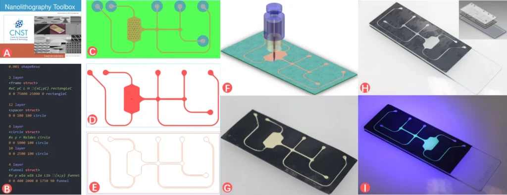
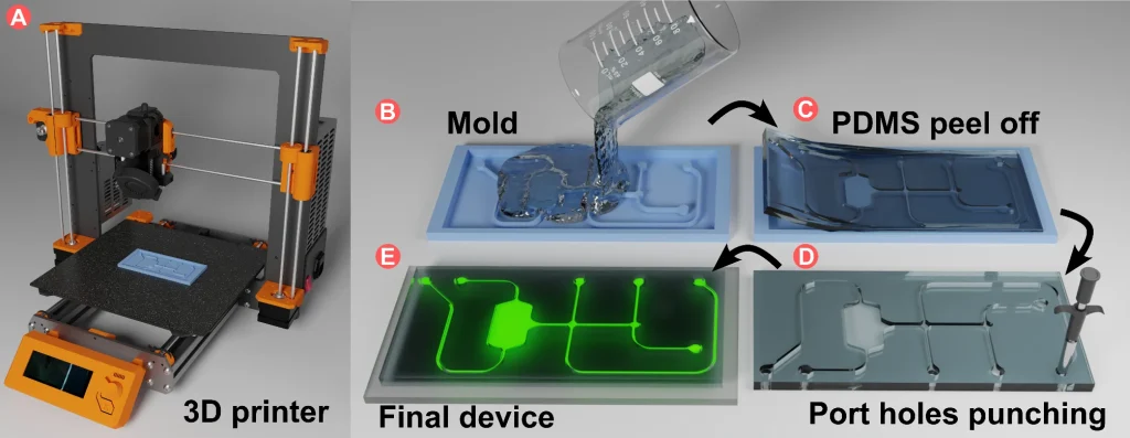 A process for manufacturing PDMS microfluidic chips
PMMA is known for its excellent optical clarity, which enhances visual inspection and optical detection capabilities. However, PMMA has poor chemical resistance to common solvents, which limits its use in water-based applications unless the microchannels are coated with polyparaxylene to improve chemical resistance and reduce molecular absorption—a technique also applicable to PDMS. PMMA chips are commonly produced using CNC milling, hot embossing, and injection molding techniques, each of which can meet different production scales and requirements. CNC milling can produce complex designs without cleanroom facilities, making it ideal for prototyping and small-batch production, but the initial setup cost is high. Hot embossing is suitable for medium and large-scale production, requiring a large upfront investment in mold making, but offers excellent detail replication. Injection molding is the best choice for large-scale production, and although the initial mold cost is higher, it can achieve scale cost benefits. The choice of PMMA chip manufacturing method depends on specific application requirements, output, and budget.
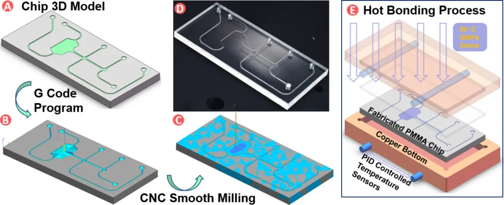 A process for manufacturing PMMA microfluidic chips
Xurography provides a cost-effective solution for rapid prototyping without cleanroom requirements using inexpensive materials such as double-sided tape. However, it lacks durability and design complexity. Due to these limitations, it is not well-suited for large-scale production.
 A process for making microfluidic chips by Xurography
Silicon-glass chips are ideal for applications that require high temperature resistance, high pressure resistance, and excellent optical properties, but their manufacturing process is complex and has many steps, requiring specialized equipment such as DRIE and clean rooms. Due to the high cost and long production time, they are not ideal for rapid prototyping or projects with limited budgets.
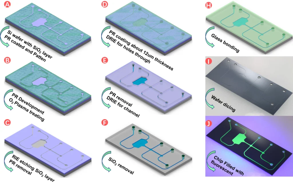 A fabrication process for silica-glass microfluidic chips
In summary, the choice of microfluidic chip fabrication method should take into account the intended application, required scalability, material and manufacturing costs, and turnaround time. For example, PDMS is cost-effective for small-scale production, with a cost of approximately $1 to $5 per chip and a turnaround time ranging from a few hours to a day depending on complexity. Although PMMA is scalable, the cost per mold ranges from $10 to $100 when prototyping, with the unit cost significantly lower during mass production. CNC milling and hot embossing have longer setup times but provide more durable chips. Xurography is the lowest-cost and fastest prototyping method, but its functionality is limited. Although silica-glass is expensive, with the cost per chip often exceeding $100 in small-scale production, it provides the best performance under harsh conditions.
Each material and method has its own strengths and is best suited for specific applications, so they should be carefully evaluated based on detailed cost analysis and functional requirements. For example, for high-precision diagnostic applications that require chemical resistance and thermal cycling durability, silica-glass is recommended. However, for teaching models and proof-of-concept designs where cost and speed are critical, Xurography or CNC-milled PMMA may be more suitable.
As the demand for rapid, reliable, and accessible diagnostic methods continues to grow, especially in response to global health challenges such as the COVID-19 pandemic, the value of highly adaptable microfluidic systems has become increasingly prominent. This paper provides the advantages and limitations of various manufacturing technologies to guide the development of next-generation microfluidic devices that can meet the evolving needs of healthcare and research.
Reference:
Liu, Xiaocheng et al. “Microfluidics chips fabrication techniques comparison.” Scientific reports vol. 14,1 28793. 20 Nov. 2024, doi:10.1038/s41598-024-80332-2
Related Services: